Hello! Today, let’s talk about a very special kind of ‘glass’ that might completely transform the future of the digital world—from the smartphones in our hands to massive AI data centers. This is the story of the ‘semiconductor glass substrate.’
This technological revolution means much more than simply ‘replacing plastic with glass.’ To truly understand it, we will embark on a journey to paint the single point of the glass substrate as a three-dimensional picture, and even as a map of the future.

Viewing the World in Three Dimensions…
First, let’s look at the glass substrate through the lens of a ‘Multidimensional Analysis Framework.’ This lens is a magical tool that allows us to observe a phenomenon simultaneously from multiple angles such as time, space, and layers.
#1. Time Axis: The Flow of Technology from Past to Future
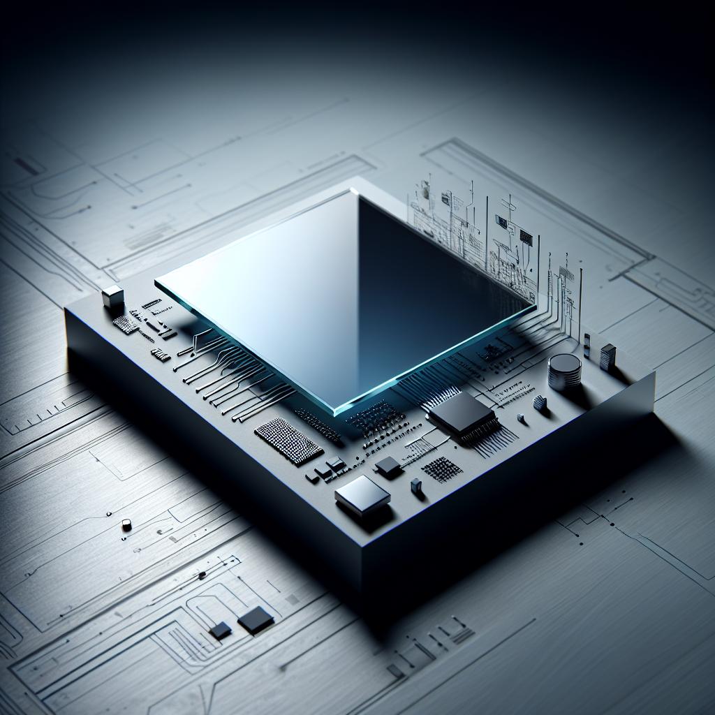
No technology just falls from the sky. The glass substrate is no exception.
- Past (The Plastic Era): For decades, the semiconductor industry developed on the solid foundation of plastic-based FC-BGA substrates. But as the massive wave of AI surged, this foundation hit its limits, bending like ‘damp pizza dough.’
- Present (Dawn of Glass): We now stand at the start of a grand project to replace the riverbed with solid bedrock—glass. Giants like Intel, Samsung Electro-Mechanics, and SKC are fiercely competing in a ‘Game of Thrones’ to seize future leadership. It’s a breathless race to overcome technical hurdles just before commercialization.
- Future (Transparent Possibilities): Once glass substrates become widespread, the flow of technology will accelerate dramatically. AI models will become hundreds of times more powerful, and laptop batteries might last for days. Perhaps after glass, new technologies like ‘optical interposers’ that transmit information with light or ‘self-healing substrates’ that repair their own circuits will emerge.
#2. Space Axis: The World Map of Technological Hegemony
This small piece of glass is redrawing the global semiconductor supply chain map.
- Rise of Domestic Companies: Samsung Electro-Mechanics and SKC (Absolics) are emerging as key players in this new market, acting as ‘fast followers’ and ‘aggressive pioneers’ respectively. This presents tremendous opportunities for the entire domestic materials, parts, and equipment ecosystem.
- War of Giants: Intel in the U.S. is trying to plant the flag of technology first, while major players like AMD and NVIDIA weigh whose side to support. The winner of this competition will not only dominate the component market but also set the ‘industry standard’ for next-generation semiconductor packaging.
- Sustainability: AI and data centers are enormous electricity consumers. The excellent power efficiency of glass substrates can reduce the environmental burden of the AI revolution, helping humanity sustain technological progress.
#3. Layer Axis: The Butterfly Effect from Microns to the Universe
Innovation in glass substrates starts in the invisible micrometer (μm) world and impacts our entire lives.
- Micro (The Battle in the Microworld): The core is the ‘TGV (Through Glass Via)’ technology. This extremely challenging process, akin to drilling tens of thousands of holes thinner than a hair in a wine glass, hinges on detecting ‘micro cracks’—the biggest obstacle to commercialization.
- Meso (Birth of a New Ecosystem): This technology demands the co-growth of a completely new supply chain ecosystem, extending beyond substrate manufacturers to special glass companies like Corning, laser equipment firms like Philoptics, and chemical material companies like Soulbrain.
- Macro (Life Changes): This micro-level innovation ultimately brings macro changes such as smarter AI, safer autonomous vehicles, and longer-lasting smartphones. Invisible foundational work is transforming the entire city of our lives.
Inventing the Future: ‘Innovative Solutions’
Now that we understand the glass substrate in three dimensions, it’s time to spread the wings of imagination. What ideas can we generate based on glass substrate technology?
#Glass Substrate, Seeds of Possibility
- Hybrid Smart Substrate: Combining the hardness of glass with the flexibility of plastic. The central part of the substrate (where high-performance chips are mounted) is made of glass to maximize performance, while the edges use flexible materials for wearable or foldable devices. 
- Self-Healing Glass Substrate: An idea to fundamentally solve the ‘micro crack’ problem, the biggest enemy of the TGV process. Using nanotechnology, microcapsules embedded in the glass release special chemicals to self-repair cracks when they occur.
Self-Healing Glass Substrate - AI-Based Process Optimization System: Developing AI that collects and analyzes all process data in real time—laser drilling, etching, deposition—to increase yield. The AI predicts micro crack formation and autonomously finds optimal process parameters, minimizing human intervention to build a smart factory.
- Lego-Style ‘Modular Substrate’: Standardizing small glass substrate modules for chiplets like CPU, GPU, and HBM. Users can easily design and build custom AI semiconductors by assembling desired modules like Lego blocks.
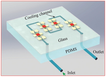
Modular Substrate - Integrated Liquid Cooling Channels: Creating ultra-fine cooling channels thinner than a hair inside the glass substrate, circulating coolant to directly dissipate heat from chips. This can dramatically solve heat issues without large fans or heatsinks.
Integrated Liquid Cooling - Transparent Display Integrated Substrate: Utilizing the transparency of glass substrates so the substrate itself acts as a micro LED display. In small devices like AR glasses or smartwatches, the processor substrate doubles as the screen, maximizing space efficiency.
- Sustainable ‘Glass Recycling’ Ecosystem: Establishing a perfect resource circulation system that efficiently recovers rare metals (copper, gold, etc.) from discarded glass substrates and reuses the remaining glass as raw material for new substrates. This supports environmental protection and creates new business models.
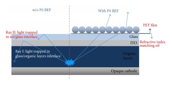
- Photonics Substrate with Integrated Optical Circuits: To overcome the limits of electrical signals, integrating optical circuits (silicon photonics) that transmit data with light alongside electrical circuits inside the glass substrate. This will raise data transmission speeds to unprecedented levels.
Photonics Substrate - Medical ‘Lab-on-a-Chip’ Platform: Using precise circuit processing and transparency of glass substrates to create ultra-small diagnostic devices that can instantly diagnose dozens of diseases from a single drop of blood. Processor, sensors, and fluid channels are integrated on one glass substrate.
- 3D Vertical Stacked Battery Using TGV: Applying TGV technology to make battery anode, cathode, and electrolyte layers as thin as hair and stacking tens of thousands vertically. This innovative idea could multiply battery capacity dozens of times in the same area.
Conclusion: A Future Built on a Transparent Foundation
Today, we explored the technology of the ‘semiconductor glass substrate.’
Advertisement
We saw that this technology is not just a simple component replacement but a massive paradigm shift shaking time, space, and the entire industrial ecosystem. It revealed the potential for us to imagine and invent an astonishing and creative future on this solid, transparent foundation.
Of course, many challenges remain—like drilling holes in a wine glass—but humanity’s challenge to open the door to the AI era will not stop. Next time you see a glass window, think about it. Beyond the transparent world we see, a solid future supporting a vast invisible digital world is growing. Glass is no longer just a window to look through but is becoming the most important foundation for building a new world.